The Semiconductor Underneath Everything
When you plug an EV into a DC fast charger, you're asking a machine to do something extraordinarily demanding: take rough AC power from the grid, convert it to high-voltage DC with sub-millivolt precision, and deliver it to a battery system — repeatedly, for years, in Indian heat and humidity, with zero tolerance for error.
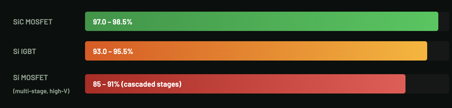
The component that makes or breaks this process is the power semiconductor switch — the transistor that switches current on and off at tens or hundreds of kilohertz to perform the AC/DC conversion. For decades, the dominant technology was the IGBT (Insulated Gate Bipolar Transistor), built on Silicon. Today, Silicon Carbide (SiC) MOSFETs are displacing IGBTs in every serious high-power application. The reasons are rooted in fundamental physics, not marketing.
10× Higher breakdown electric field vs Silicon
3× Higher thermal conductivity vs Silicon
<100ns Switching transient times in SiC devices
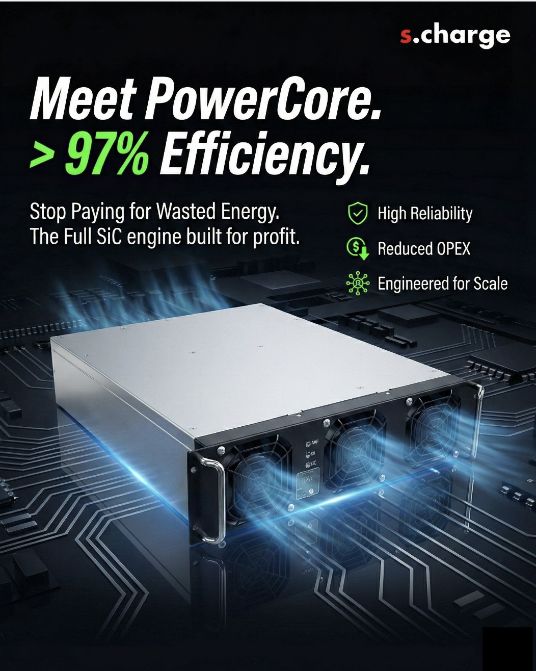
SCharge Full SiC PowerCore - The Engine the power SCharge DC Fast Chargers
Si Mosfet vs IGBT vs SiC — A Physics-First Comparison
Si MOSFET: the original workhorse
Silicon MOSFETs dominated low-voltage power conversion for decades. They switch fast, are inexpensive to manufacture, and perform admirably below ~200V. However, their on-state resistance (RDS(on)) rises steeply with voltage rating due to the relatively low breakdown field of silicon. At 600V–1200V ratings — the range that DC fast chargers operate in — a Silicon MOSFET's on-state resistance becomes impractically high, requiring enormous parallel die configurations that are costly, thermally complex, and ultimately still lossy at the currents a DC charger demands.
IGBTs: solving voltage at the cost of switching speed
The IGBT was developed precisely to address this. By combining bipolar minority-carrier conduction with a MOSFET gate structure, IGBTs achieve a low on-state saturation voltage (VCE(sat)) even at 600V, 1200V, and 1700V ratings. This made them the dominant device for motor drives, inverters, and first-generation EV chargers worldwide.
But IGBTs carry a fundamental trade-off: the minority carriers injected for low conduction loss must be swept out during turn-off. This creates a characteristic current tail — a sluggish period where current continues flowing as stored charge clears from the silicon lattice. This tail limits practical switching frequencies to 10–20 kHz. Beyond that, switching losses escalate faster than efficiency gains from better magnetics, making it impractical to go higher.
Silicon also imposes a hard thermal ceiling. Its bandgap of 1.1 eV means junction temperatures above 150–175°C are reliably destructive. In a 60–300 kW DC charger conducting hundreds of amperes, managing this thermal constraint becomes the single most expensive design problem — demanding large heatsinks, forced-air or liquid cooling loops, and conservative derating.
SiC MOSFETs: a different material universe
Silicon Carbide (4H-SiC specifically) operates in a fundamentally different physical regime. Its bandgap is 3.26 eV — nearly three times silicon's. This single material property cascades through the entire device and system design:
| Parameter | Si MOSFET | Si IGBT | SiC MOSFET |
| Bandgap | 1.1 eV | 1.1 eV | 3.26 eV |
| Max junction temperature (Tj) | 150–175°C | 150–175°C | 200–225°C |
| Practical switching frequency | 20–200 kHz (low V only) | 5–20 kHz | 50–500 kHz |
| Switching losses at 100 kHz | N/A at high voltage | Very high (impractical) | Very low |
| Reverse recovery charge (Qrr) | Low–moderate | High (freewheeling diode) | Near-zero |
| Thermal conductivity | 1.5 W/m·K | 1.5 W/m·K | 4.9 W/m·K |
| Body diode turn-off tail | Present | No intrinsic body diode | Negligible — no minority carriers |
| On-state loss at 1200V | Impractical (high RDS) | Moderate (VCE(sat)) | Low (unipolar conduction) |
| Temperature coefficient of Ron | Positive (worsens at heat) | Complex (bipolar) | Mild positive — stable behaviour |
The Qrr Insight
The near-zero reverse recovery charge of SiC MOSFETs eliminates the dominant dynamic switching loss in bridge converter topologies. In IGBT-based designs, every time a freewheeling diode recovers at the end of its conduction period, a destructive current spike flows backward through it. In a 150 kW charger running at 20 kHz, this reverse recovery loss alone accounts for 3–5 kW of continuous heat dissipation. SiC reduces this to near-zero — improving both efficiency and reliability simultaneously.
Understanding Ripple — and Why It Directly Affects Battery Health
When an AC/DC power converter produces its output "DC" voltage, it isn't perfectly flat. Residual AC components ride on top of the DC level — this is ripple. It has two measurable dimensions: voltage ripple (periodic variation in output DC voltage) and current ripple (AC current superimposed on the DC current entering the battery).
Voltage ripple (ΔV)
Periodic fluctuation in output DC voltage, expressed as a percentage of nominal Vout or in peak-to-peak millivolts. High-quality chargers target <0.5% peak-to-peak. Excessive ripple stresses the battery BMS overvoltage monitoring circuits and can trigger nuisance protection trips during high-SoC charging. More critically, it causes periodic micro-overcharge of cells, accelerating SEI layer growth and lithium plating at the anode.
Current ripple (ΔI)
AC current flowing into the battery cell superimposed on the DC charge current. This causes resistive heating inside cells (I²R in the cell's internal resistance), electrochemical cycling stress on the electrode interfaces, and at low frequencies, partial lithium intercalation and de-intercalation on every cycle. Industry benchmark for high-quality chargers is <2% of rated charge current at the BMS terminals.
The physics of ripple and switching frequency
Ripple amplitude is fundamentally governed by the output filter — specifically the inductance (L) and capacitance (C) of the LC stage at the converter output. The ripple current in an output inductor is described by:
Fundamental Ripple Equation
ΔIL = (Vin − Vout) × D ÷ (L × fsw)
Ripple is inversely proportional to switching frequency. A SiC converter operating at 100 kHz produces 5× less inductor ripple current than an equivalent IGBT design at 20 kHz — with exactly the same inductor. Alternatively, you can use a 5× smaller inductor for equivalent ripple performance. This cascades directly into smaller, lighter magnetics, faster transient response, and smaller output capacitor banks.
In practice, a 150 kW IGBT-based charger typically requires 4–8 large electrolytic capacitors providing 40,000–80,000 µF of output capacitance to manage ripple. An equivalent SiC design at 100+ kHz achieves superior ripple specification with 500–2,000 µF of metallised polypropylene film capacitors — components with dramatically lower ESR, far higher reliability, no electrolyte degradation over temperature, and rated for 100,000+ hours of operation.
The reduction in ripple current entering the battery is not merely about compliance. Research from multiple battery laboratories shows that AC ripple current at 20–40 kHz (the switching harmonic frequency of IGBT converters) penetrates cell chemistry more aggressively than ripple at 200–400 kHz (the harmonic range of SiC converters), where the cell's internal inductance provides natural attenuation. Less ripple current = slower capacity fade = longer battery warranty support = lower fleet replacement costs.
Voltage Regulation — Precision Under Dynamic Load
A DC charger is not delivering power into a fixed resistive load. It is powering a battery system whose effective impedance changes continuously with state of charge, temperature, cell chemistry ageing, and the BMS charge protocol. The charger must maintain tight voltage regulation — typically within ±0.5% of setpoint — across a wide load range and during rapid transitions in the CC/CV charging profile.
The control bandwidth problem
A voltage regulation control loop cannot respond faster than approximately one-tenth of the switching frequency. An IGBT converter switching at 20 kHz has a practical control bandwidth ceiling of roughly 2 kHz. This is adequate for slow, steady-state charging — but insufficient during the abrupt current step-changes commanded by the BMS during thermal protection events, near full SoC, or multi-gun power sharing rebalancing. The result is voltage overshoot or undershoot at the output terminals during transitions.
A SiC converter switching at 150 kHz has a control bandwidth exceeding 15 kHz — more than 7× wider. This translates to:
Fast transient recovery
When the vehicle BMS commands a sudden step from 80A to 20A, the charger restores its voltage setpoint in under 100 µs rather than 500+ µs. Less voltage overshoot, reduced risk of BMS protection activation, and smoother energy delivery to the cell stack.
Better static regulation accuracy
Tighter DC setpoint accuracy from 5% to 100% rated load. Critical for multi-gun dynamic power sharing architectures where output current on each gun changes continuously based on vehicle demand profiles across the charger array.
Relevance to Indian Grid Conditions
India's distribution grid — particularly in Tier 2/3 cities, industrial areas, and highway corridor substations — is characterised by frequent voltage fluctuations: sags to 170–190V single phase, brief swells, and harmonic pollution from adjacent industrial loads. IGBT converters with slow PFC loop bandwidth can struggle to maintain output stability and unity power factor during these events, causing charging interruptions or nuisance protection trips. SiC-based high-frequency PFC stages maintain stable regulated output and power factor above 0.99 through grid disturbances that would destabilise legacy designs.
Current Regulation — Protecting Every Cell in the Pack
Current regulation in a DC fast charger operates at two distinct levels: the macroscopic DC current setpoint command (the CC phase of CC/CV charging), and the suppression of microscopic AC ripple current at the cell terminal. Both are critical for battery longevity — and both improve dramatically with SiC technology.
CC phase accuracy
During constant-current charging, the charger must maintain output current within typically ±1% of the commanded value across the full output voltage range — often 200V to 1000V for a modern 800V-platform charger. Poor current regulation accuracy causes overcharge risk at high SoC or underdelivery at low SoC. The high control bandwidth of SiC converters maintains current regulation even during rapid input voltage variations, which are common in weak-grid installations without line conditioning infrastructure.
Ripple current and cell ageing
Battery researchers have consistently demonstrated that AC ripple current superimposed on DC charge current accelerates capacity fade through multiple mechanisms: increased internal heating (I²R in the cell impedance), periodic lithium plating at the anode during current peaks, SEI layer growth from electrochemical cycling at the interfaces, and electrode mechanical fatigue from volume expansion and contraction at the ripple frequency.
The effect is frequency-dependent and strongly favours higher-frequency ripple. At 20–40 kHz (IGBT converter harmonic range), the cell impedance is relatively low and ripple current penetrates deeply into the chemistry. At 200–400 kHz (SiC converter harmonic range), cell internal inductance rises and effectively blocks the ripple — the current "seen" by the electrode chemistry is orders of magnitude lower, even if the total ripple amplitude at the terminals is similar. SiC-based converters thus extend battery cycle life not only through lower absolute ripple amplitude, but through pushing remaining ripple to frequencies the battery itself can reject.
Typical Peak Efficiency: Where Physics Becomes Rupees and Emissions
Efficiency is the commercially decisive specification of a DC fast charger — more impactful than raw power rating in determining total cost of ownership. Every percentage point of efficiency lost becomes heat that must be managed, and electricity purchased from the grid without being delivered to vehicles. Over a 10-year charger life at Indian industrial tariffs, these losses compound to crores of rupees.
The compounding economics of a 3% efficiency gap
Consider a 150 kW DC fast charger operating 16 hours per day at 60% average utilisation — a reasonable high figure for a highway corridor or fleet depot but still used for calculations. Compare an IGBT design at 94% efficiency against a SiC design at 97.5%:
Annual Energy Economics — 150 kW DC Fast Charger
Assumptions: 16 hrs/day operation, 60% utilisation, ₹9/kWh blended commercial tariff
Daily vehicle-side energy delivered 864 kWh
IGBT design — daily grid draw (÷0.94) 919 kWh
SiC design — daily grid draw (÷0.975) 886 kWh
Daily excess grid energy — IGBT vs SiC33 kWh/day wasted
Annual additional electricity cost (IGBT)≈ ₹1,08,000 / year / charger
10-charger depot over 10 years≈ ₹1.08 Crore additional grid spend
SiC premium payback — energy savings alone< 18–24 months
*- The above calculation can be done as per actual utilisation.
This analysis excludes cooling infrastructure savings — which are equally significant. A 150 kW IGBT charger dissipates 9–10 kW of heat at full load. A SiC equivalent dissipates 3.75–6 kW. That 4–6 kW difference means smaller heatsinks, reduced or eliminated liquid cooling loop pump power, lower cabin air conditioning loads (in sealed enclosures), and dramatically extended life of thermal interface materials and cooling system components.
In Maharashtra's climate, where ambient temperatures regularly reach 40–45°C at charging sites, this thermal reduction is not merely an efficiency metric. It is the difference between a charger that operates continuously at rated power and one that derates to 60–70% on hot afternoons — exactly when highway and fleet charging demand peaks.
Arrhenius Reliability Multiplier
Every 10°C reduction in semiconductor junction temperature approximately doubles the device MTBF (Mean Time Between Failures) according to the Arrhenius reliability model. SiC's lower switching losses and 3× higher thermal conductivity, combined, can reduce steady-state junction temperature by 30–50°C compared to an equivalent IGBT design at the same thermal management spend. By the Arrhenius model, this translates to an 8–32× improvement in power semiconductor longevity — directly reducing maintenance costs and unplanned downtime.
Power Quality: PFC, Harmonics, and Grid Partnership
A DC fast charger is not merely a passive load on the distribution grid. It is an active grid participant whose power quality behaviour determines the health of the shared infrastructure it connects to. Poor power quality from charging hardware creates measurable harmonic distortion on local LT/MV networks, reduces transformer efficiency, increases neutral current in three-phase installations, and can violate IEC 61000-3-2 and IEEE 519 harmonic compliance limits — triggering DISCOM penalties or forced derating requirements.
SiC-based Active Front End (AFE) rectifiers with high-frequency PFC achieve Total Harmonic Distortion (THD) below 3% and displacement power factor above 0.99 across the full load range from 10% to 100%. IGBT-based designs typically operate at 5–15% THD and 0.90–0.95 power factor at partial loads — the operating condition that dominates actual average utilisation.
For operators connecting multiple fast chargers to a shared distribution transformer — a bus depot, a logistics warehouse, a multi-unit charging hub — this difference determines whether the installation requires expensive harmonic filter banks, transformer derating compensation, or APFC panels. These remediation costs regularly exceed the semiconductor premium by multiples.
SiC in the DC Charger Architecture: Where It Lives
Modern isolated DC fast chargers consist of multiple power conversion stages. SiC devices transform the performance of each:

AC/DC PFC front end
Totem-pole or Vienna rectifier topology or other topologies. SiC eliminates slow anti-parallel diode recovery, enabling bridgeless operation with power factor >0.99, THD <3%, and >98% efficiency in the front-end stage alone.
Isolated DC/DC stage
Dual Active Bridge (DAB) or LLC resonant topology. SiC at 100–300 kHz enables transformers 5–10× smaller than IGBT designs. Ideal for liquid-cooled module stacking in high-power chargers above 120 kW.
Synchronous rectification
SiC body diode near-zero reverse recovery eliminates the largest single loss mechanism in high-frequency secondary-side rectification, cutting output stage losses by 60–80% vs IGBT + external diode combinations.
How SCharge Brings This to Life
SCharge designs and manufactures AC and DC EV charging hardware from Nashik — built ground-up for Indian grid conditions, Indian heat, and the precision that modern EV fleets demand. Our power electronics choices are deliberate, not catalogue-sourced.
D1 Series — 60 to 360 kW DC Fast Charger
Modular DC fast chargers with SiC-based power modules. Designed for 97%+ efficiency at full load in 45°C ambient. Air and liquid-cooled options. CCS2, Onboard OCPP with real-time efficiency and power quality telemetry to the SCharge NOC & Customer CMS.
BESS + V2G Bidirectional Chargers
SiC bidirectional converters enable seamless grid-to-vehicle, vehicle-to-grid, and vehicle-to-building power flow on a unified 800V DC bus. The same semiconductor platform that charges can dispatch stored energy to the grid during peak tariff periods — turning a charging hub into a revenue-generating asset.
SCharge CMS — Cloud Charge Management
Real-time per-session monitoring of charger efficiency & power quality metrics. Fleet operators receive precise energy accuracy reporting for cost attribution and can detect degraded power quality conditions before they affect battery assets or trigger DISCOM compliance events.
Our engineering team actively designs and tests SiC-based power conversion stages in Nashik — from DAB transformer construction using nanocrystalline amorphous cores, to C-state-machine thermal derating firmware for BESS modules, to insulation monitoring for high-voltage DC bus systems. This is system-level engineering, not component reselling. It's the infrastructure India's EV transition demands — built by engineers who understand both the power electronics and the deployment reality.

Conclusion: The Semiconductor Choice Is the System Choice
The transition from Silicon/IGBT to Silicon Carbide in EV charging power electronics is not an incremental improvement — it is a categorical shift across every dimension that matters for operators, fleets, and grid operators. Higher switching frequency enables smaller passive components and dramatically lower ripple. Lower switching losses enable higher efficiency and reduced thermal burden. Superior thermal conductivity and higher rated junction temperature improve reliability in harsh environments. The near-zero body diode reverse recovery eliminates the dominant dynamic loss mechanism in converter bridge topologies.
For fleet operators, CPOs, and infrastructure developers evaluating DC charger procurement, the semiconductor technology inside the enclosure is the specification that determines long-run economics — not nameplate power, not sheet metal colour. A SiC-based charger operating at 97.5% efficiency will outperform, outlast, and undercost a legacy IGBT design at 94% over any realistic deployment horizon in India's operating environment.
The physics is clear. The operating economics confirm it. SiC is the right technology for serious EV charging infrastructure — and it is at the core of every high-power product SCharge makes.
Testing at SCharge
"We do what we say, we say what we mean, and we mean what we do."
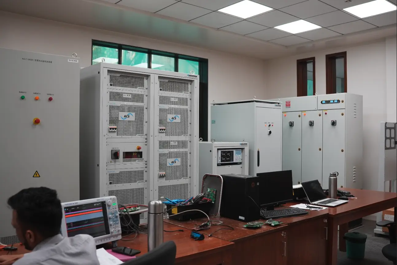
At SCharge, our power electronics validation goes beyond datasheet compliance. Our engineering team conducts AC/DC grid simulation and power quality testing using professional-grade equipment including the Regatron grid simulator and DC Simulation platform — enabling full programmable recreation of Indian grid conditions: voltage sags, swells, harmonic injection, and frequency deviations, all applied to our converter front ends under live load conditions. Output power quality and waveform accuracy are characterised using the Yokogawa WT5000 precision power analyser, capturing efficiency curves, THD, power factor, and ripple metrics with sub-0.1% measurement uncertainty. This level of test rigour — typically found in accredited NABL or tier-1 OEM labs — is part of how SCharge validates every major design revision before a single unit ships to a customer site.
AC/DC Simulation
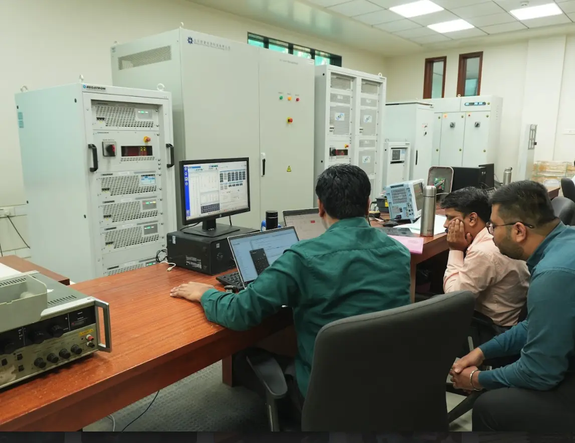
Analysis on WT5000 Analyser
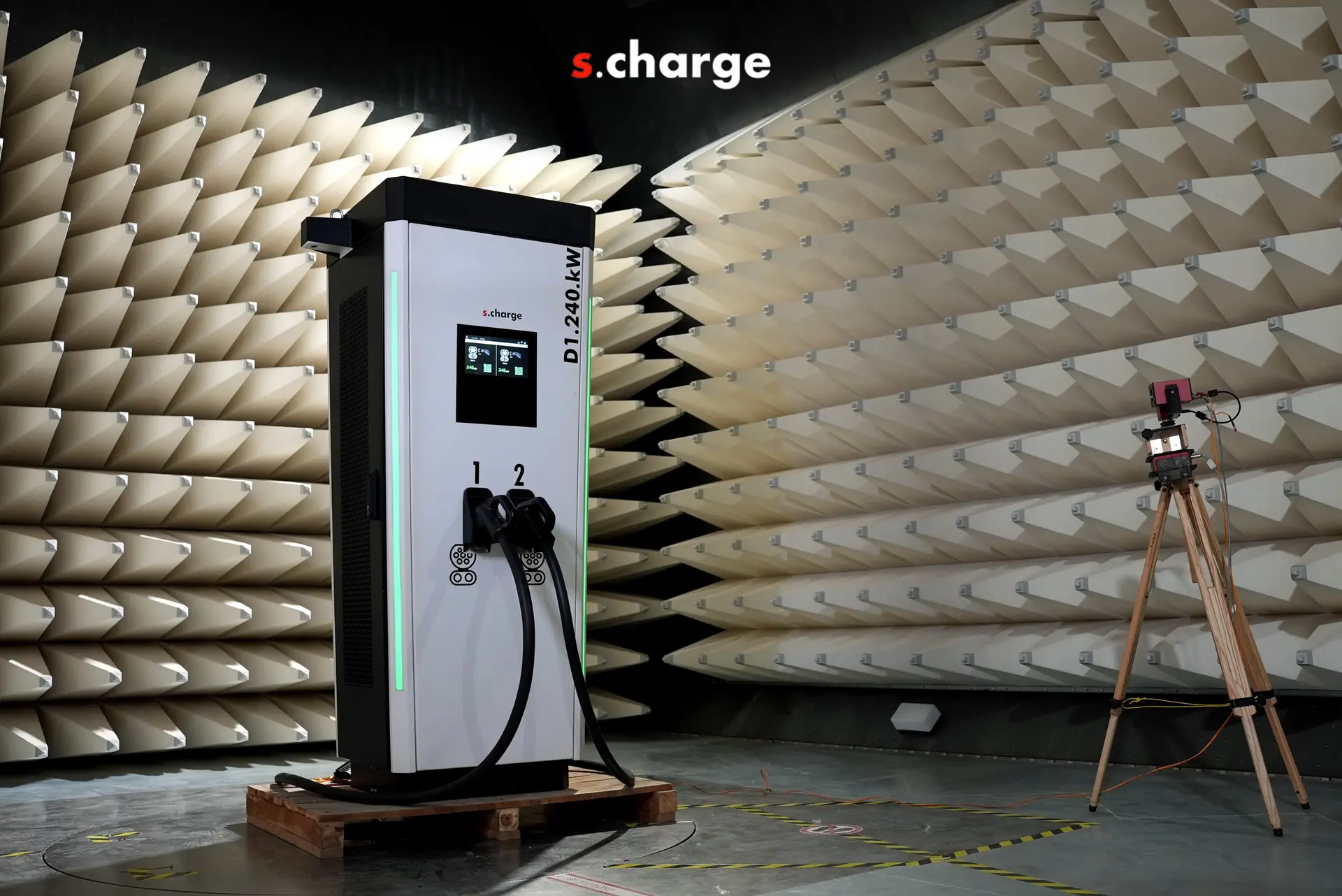
EMI/EMC Testing
#SCharge Power Core #Full SiC #High Efficiency Power Modules